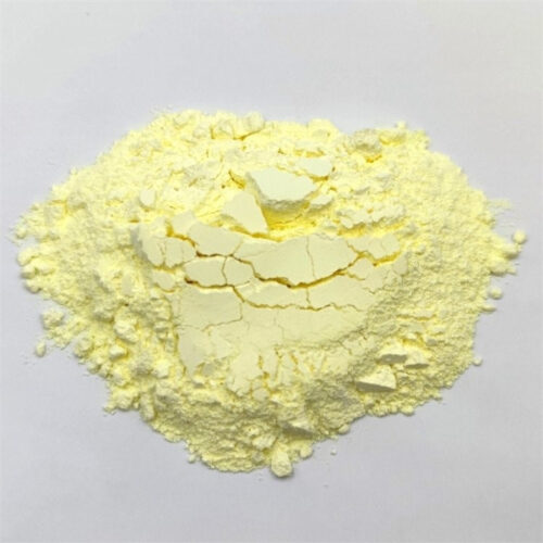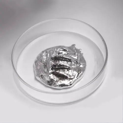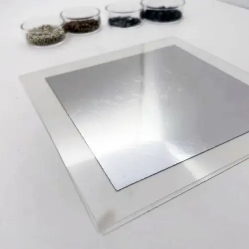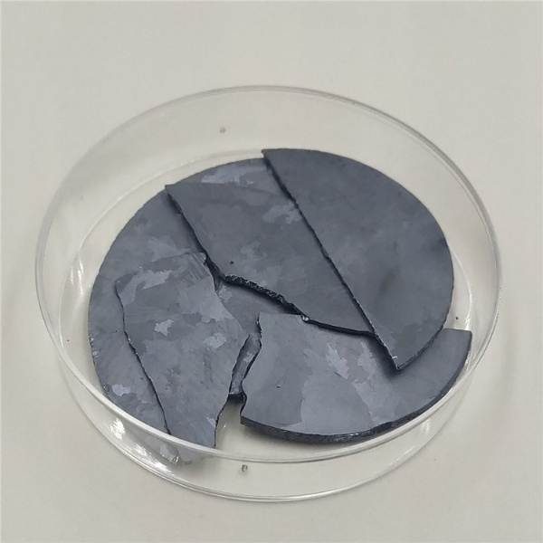
Indium phosphide (InP) is a compound of phosphorus and indium, renowned for its excellent semiconductor properties. Semiconductor devices manufactured using indium phosphide substrates exhibit high saturated electron drift velocity, suitable emission wavelengths for low loss fiber optic communication, strong radiation resistance, good thermal conductivity, high photoelectric conversion efficiency, and a relatively high bandgap width. Consequently, indium phosphide substrates are widely used in manufacturing optical module devices, sensor devices, high-end radio frequency devices, etc.
| Product Name | Indium Phosphide, InP |
| Puriy | 99.999% |
| Crystal Structure | Zinc blende |
| Melting Point | 1,062 °C |
| Cas No. | 22398-80-7 |
| Molar Mass | 145.792 g/mol |
| Density | 4.81 g/cm3, solid |
| Band Gap | 1.344 eV |
| Electron Mobility | 5400 cm2/(V·s) (300 K) |
| Thermal Conductivity | 0.68 W/(cm·K) (300 K) |
Indium phosphide (InP) is an important compound semiconductor material with several advantages, including high saturated electron drift velocity, strong radiation resistance, good thermal conductivity, high photoelectric conversion efficiency, and a high bandgap width. InP has a zinc blende crystal structure with a bandgap of 1.34 eV and a mobility ranging from 3000 to 4500 cm2 /(V.S)at room temperature. It is widely applied in optical communication, high-frequency millimeter-wave devices, optoelectronic integrated circuits, and solar cells used in outer space. Given these material properties, semiconductor devices manufactured with indium phosphide substrates are extensively utilized in the production of radio frequency devices, optical modules, LEDs (including Mini LEDs and Micro LEDs), lasers, detectors, sensors, and space solar cells. They have broad applications in fields such as 5G communications, data centers, next-generation displays, artificial intelligence, autonomous driving, wearable devices, and aerospace.
Indium phosphide semiconductor materials feature a wide bandgap structure, and electrons travel at high speeds through InP material. As a result, satellite signal receivers and amplifiers made with indium phosphide chips can operate at extremely high frequencies above 100 GHz, with wide bandwidth, minimal external interference, and high stability. Therefore, indium phosphide is a more advanced semiconductor material than gallium arsenide, potentially driving the satellite communications industry to develop into higher frequency bands.
Compared with gallium arsenide (GaAs), indium phosphide (InP) demonstrates prominent advantages in electrical and other physical properties, holding a dominant position in the semiconductor optical communication field. Compared to GaAs, indium phosphide has the following advantages: (1) It offers high electron peak drift velocity, a high bandgap width, and high thermal conductivity. InP has a direct transition bandgap of 1.34 eV, which corresponds to the wavelength with the least transmission loss in optical communication; its thermal conductivity is higher than that of GaAs, leading to better heat dissipation. (2) Indium phosphide is more advantageous than GaAs in device fabrication. InP devices feature a high current peak-to-valley ratio, determining high conversion efficiency; InP’s momentum energy relaxation time constant is half that of GaAs, leading to a working efficiency limit twice that of GaAs devices; InP devices have better noise characteristics. (3) Indium phosphide (InP) as a substrate material has the following primary applications: optoelectronic devices, including light sources (LEDs) and detectors (APD avalanche photodetectors), mainly used in fiber optic communication systems; integrated lasers, photodetectors, and amplifiers are essential components in optoelectronic integrated circuits for the next-generation 40 Gb/s communication systems.